Machine-Learning Based Solution to Detect Defects In Semiconductor Manufacturing Process
Machine-Learning Based Solution to Detect Defects In Semiconductor Manufacturing Process
- Technology : Artificial Intelligence, Deep Learning, Image Processing & Computer Vision
- Industry : Manufacturing

Business Objective
Today’s semiconductor manufacturers face many challenges and one of the significant ones is the visual inspection process of the wafer surface in manufacturing. It is also important to consider here that with advancements in semiconductor processing technologies, each part is becoming more complex and denser.
This solution is designed to meet the growing demands in the semiconductor manufacturing industry by automating manual inspection using machine learning. The goal of this system is to detect and classify wafer detects to improve the accuracy and efficiency of the detection identification process. It replaces time-consuming and erroneous processes with accurate and faster detection identification processes. This will ultimately lead to a reduction in production costs and an increase in the quality of the final product. These detects, if left unnoticed, can cause significant losses. This solution helps manufacturers carefully inspect different types of detects along with their position on the wafer surface.
Solution
The proposed solution is designed to detect surface defects on semiconductor wafers. It uses deep learning methods to find out types of detects accurately.
The system works by analyzing the digital images of the wafer surface and comparing them to a pre-existing database of known defect patterns. It uses neural network models to identify and classify the defects based on their shape, size, and location on the wafer surface.
The solution can detect 32 categories of detecting with nine primary detects. One of the main features of this solution is it is capable to recognize two-mix-categories errors that might go unnoticed in such solutions. It is designed in a way that it can continue to improve its accuracy over time, leading to greater efficiency gains.
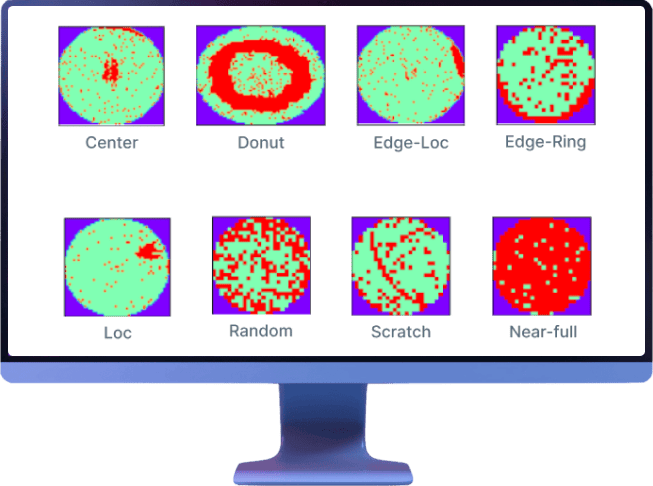
Once deployed, it categorizes For example, It detects edge-ring, donuts, scratches, and center detects shown in the figure below. It also recognizes a combination of two types of detects effectively which makes a difference compared to other detection solutions.
Result
By implementing this solution, semiconductor manufacturers can achieve faster and more accurate wafer inspection. The system can process large quantities of wafer images in a short amount of time, reducing the need for manual inspection and allowing for faster production cycles. Additionally, the system’s ability to learn and adapt means that it can continue to improve its accuracy over time.
Benefits
The benefits of adopting a machine-learning-based solution for wafer defect detection and categorization are numerous. First and foremost, the system can improve the quality of the final product by identifying and addressing defects that might otherwise go unnoticed. This can lead to reduced product returns.
In addition, the system can reduce production costs by streamlining the inspection process and reducing the need for manual labor. This can lead to improved production efficiency and faster time to market. It helps manufacturers meet the growing demands by automating the detection of defects. By adopting machine-learning-based solutions, manufacturers can achieve a high level of accuracy and speed to improve the yield.
Connect With Us To Leverage Data For Insights And Intelligence
Crafting Data Success Stories
Secure Data Migration Journey For A Leading Construction Company

QlikView To Microsoft Power BI Migration

Comprehensive Healthcare Survey Application with Omni-Channel Capabilities

Our Source of Motivation


